PCB Fabrication
Here at The Hive, we have a suite of tools made by LPKF that enable students to fabricate printed circuit boards (PCBs). Students go through a three-step training process to gain access to the tools, after which they can use the equipment and our materials free of charge whenever The Hive is open.
The Hive provides double-sided copper on FR4 in 0.5 oz/ft² (18 um) and 1 oz/ft² (35 um) weights to our users at no cost, though many other substrates can be used.
A detailed guidebook for how to fabricate PCBs using the two tools is located at the ProtoMat. Stencil fabrication information can be found in the guidebook at the ProtoLaser.
There are two primary pieces of equipment used in this process:
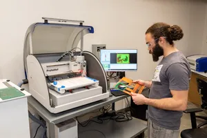
- The LPKF ProtoMat S103 - a 2.5-dimensional plotter that drills and mills (cuts) PCB substrates, plastics, and soft metals
- The LPKF ProtoLaser U4 - a 20um-diameter laser to etch (selectively remove) a wide variety of film/substrate pairings
If you need vias, which are usually achieved via electroplating, we suggest looking for alternative options, such as 1mm through-holes or no-via designs.
- To make vias in our no-plating process, make any vias as 1mm-diameter holes (excluding the annular ring), and then solder in a standard header pin.
- Otherwise, your best option is likely to get it fabricated professionally; see our PCB Design page for some fabrication house options.
We also can cut stencils from polyamide or PET sheets (for stainless, see the laser cutting area), and assemble boards with a reflow oven. We also have a few unsupported capabilities, including applying soldermask and silkscreen, a less-complicated psuedo-masking process, as well as a chemical-free electroplating process, but again, your mileage may vary with these. Head to our PCB fabrication page for more details.
Our DRC file: DRC
Out CAM file: CAM
Quick Links
- No idea what a trace is? –> What is a PCB?
- Designing your own PCB? –> PCB Design
- What can we do, and how to do it –> PCB Fabrication
- It’s suggested that if you’re having processing issues, go to the relevant process guide first to confirm you’re doing things right.
- Then look at the relevant tool pages (Protomat, Protolaser) for additional details.
- Looking to take your fab to the next level? –> Tips, tricks, and process miscellany
Questions? You can reach the PCB MPIs at hive-pcb@ece.gatech.edu.